← 返回列表
🔗 原文
High-Density Parchment Paper Papertronics with Laser-Carved Hydrophilic Channels

Paper as a substrate for electronic circuits is not very common, but promising for flexible circuits with low cost and easy recyclability. That said, paper is not an easy material to work with when printing traces, as the cellulose material is both absorbent and irregular, limiting the resolution and accuracy of so-called papertronics. Even when using higher-quality paper with wax-based masks this resulted in poor resolution issues, so [Zahra Rafiee] et al. opted to approach the problem from the other direction, by using hydrophobic parchment paper as the base combined with a laser.

The nice thing about the inks used with papertronics that they aren’t just traces, but can also be functional elements like resistors, which is also demonstrated in the paper. The channels for the inks are created using a 50 Watt CO2 laser, which etches away the silicone coating on the parchment paper. The achieved resolution in the article is around 250 µm for line widths and 300 µm line spacing, which is much better than that for wax-based alternatives.

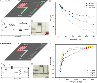
Providing conductivity in the inks was PEDOT:PSS, which, when mixed with dimethyl sulfoxide (DMSO), creates resistors. Capacitors can be printed by creating interlocking PEDOT:PSS ‘fingers’, with a Poly Vinyl Alcohol (PVA) based gel overlaid as electrolyte. These combinations were used to create RC low- and high-pass filters.

The degradation of these papertronic circuits was also tested, with them buried in soil under typical conditions. Only the silicone coating was rather immune to degradation. Since silicone is considered chemically and biologically inert, it’s claimed to not be an issue. For situations where such easy decomposition is not desirable, encapsulation with polydimethylsiloxane (PDMS) is offered as an option.

🤖 AI 总结
本文介绍一种以羊皮纸为基底、激光雕刻亲水通道的高密度纸质电子技术,利用纸的柔性、低成本和可回收性,克服了纸基材料加工难题。

Paper as a substrate for electronic circuits is not very common, but promising for flexible circuits with low cost and easy recyclability. That said, paper is not an easy material to work with when printing traces, as the cellulose material is both absorbent and irregular, limiting the resolution and accuracy of so-called papertronics. Even when using higher-quality paper with wax-based masks this resulted in poor resolution issues, so [Zahra Rafiee] et al. opted to approach the problem from the other direction, by using hydrophobic parchment paper as the base combined with a laser.

The nice thing about the inks used with papertronics that they aren’t just traces, but can also be functional elements like resistors, which is also demonstrated in the paper. The channels for the inks are created using a 50 Watt CO2 laser, which etches away the silicone coating on the parchment paper. The achieved resolution in the article is around 250 µm for line widths and 300 µm line spacing, which is much better than that for wax-based alternatives.

Providing conductivity in the inks was PEDOT:PSS, which, when mixed with dimethyl sulfoxide (DMSO), creates resistors. Capacitors can be printed by creating interlocking PEDOT:PSS ‘fingers’, with a Poly Vinyl Alcohol (PVA) based gel overlaid as electrolyte. These combinations were used to create RC low- and high-pass filters.

The degradation of these papertronic circuits was also tested, with them buried in soil under typical conditions. Only the silicone coating was rather immune to degradation. Since silicone is considered chemically and biologically inert, it’s claimed to not be an issue. For situations where such easy decomposition is not desirable, encapsulation with polydimethylsiloxane (PDMS) is offered as an option.

原文
High-Density Parchment Paper Papertronics with Laser-Carved Hydrophilic Channels

Paper as a substrate for electronic circuits is not very common, but promising for flexible circuits with low cost and easy recyclability. That said, paper is not an easy material to work with when printing traces, as the cellulose material is both absorbent and irregular, limiting the resolution and accuracy of so-called papertronics. Even when using higher-quality paper with wax-based masks this resulted in poor resolution issues, so [Zahra Rafiee] et al. opted to approach the problem from the other direction, by using hydrophobic parchment paper as the base combined with a laser.

The nice thing about the inks used with papertronics that they aren’t just traces, but can also be functional elements like resistors, which is also demonstrated in the paper. The channels for the inks are created using a 50 Watt CO2 laser, which etches away the silicone coating on the parchment paper. The achieved resolution in the article is around 250 µm for line widths and 300 µm line spacing, which is much better than that for wax-based alternatives.

Providing conductivity in the inks was PEDOT:PSS, which, when mixed with dimethyl sulfoxide (DMSO), creates resistors. Capacitors can be printed by creating interlocking PEDOT:PSS ‘fingers’, with a Poly Vinyl Alcohol (PVA) based gel overlaid as electrolyte. These combinations were used to create RC low- and high-pass filters.

The degradation of these papertronic circuits was also tested, with them buried in soil under typical conditions. Only the silicone coating was rather immune to degradation. Since silicone is considered chemically and biologically inert, it’s claimed to not be an issue. For situations where such easy decomposition is not desirable, encapsulation with polydimethylsiloxane (PDMS) is offered as an option.

中文翻译
High-Density Parchment Paper Papertronics with Laser-Carved Hydrophilic Channels

翻译尚未生成